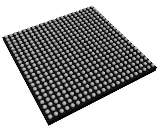
EP3CLS100U484C7N

EP3CLS100U484C7N
Mfr. #:
EP3CLS100U484C7N
Hersteller:
Intel / Altera
Beschreibung:
FPGA - Field Programmable Gate Array FPGA - Cyclone III 6278 LABs 294 IOs
Lebenszyklus:
Neu von diesem Hersteller.
Datenblatt:
EP3CLS100U484C7N Datenblatt
Die Zustellung:
DHL FedEx Ups TNT EMS
Zahlung:
T/T Paypal Visa MoneyGram Western Union
HTML Datasheet:
EP3CLS100U484C7N DatasheetEP3CLS100U484C7N Datasheet (P4-P6)EP3CLS100U484C7N Datasheet (P7-P9)EP3CLS100U484C7N Datasheet (P10-P12)EP3CLS100U484C7N Datasheet (P13-P14)
ECAD Model:
Mehr Informationen:
EP3CLS100U484C7N Mehr Informationen EP3CLS100U484C7N Product Details
Produkteigenschaft
Attributwert
Hersteller:
Intel
Produktkategorie:
FPGA - Feldprogrammierbares Gate-Array
RoHS:
Y
Produkt:
Zyklon III LS
Anzahl der Logikelemente:
100448
Anzahl der Logik-Array-Blöcke - LABs:
6278
Anzahl I/Os:
294 I/O
Betriebsversorgungsspannung:
1.15 V to 1.25 V
Minimale Betriebstemperatur:
0 C
Maximale Betriebstemperatur:
+ 70 C
Montageart:
SMD/SMT
Paket / Koffer:
BGA-484
Verpackung:
Tablett
Serie:
Cyclone III EP3CLS100
Marke:
Intel / Altera
Maximale Betriebsfrequenz:
274 MHz
Feuchtigkeitsempfindlich:
ja
Produktart:
FPGA - Feldprogrammierbares Gate-Array
Werkspackungsmenge:
84
Unterkategorie:
Programmierbare Logik-ICs
Gesamtspeicher:
4451328 bit
Handelsname:
Zyklon III
Tags
EP3CLS100U484C, EP3CLS100U, EP3CLS10, EP3CLS1, EP3CL, EP3C, EP3
Service Guarantees

We guarantee 100% customer satisfaction.

Quality Guarantees

We provide 90-360 days warranty.

If the items you received were not in perfect quality, we would be responsible for your refund or replacement, but the items must be returned in their original condition.
Our experienced sales team and tech support team back our services to satisfy all our customers.

we buy and manage excess electronic components, including excess inventory identified for disposal.
Email us if you have excess stock to sell.

Email: [email protected]
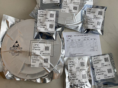
Step1: Vacuum Packaging with PL
Step1:
Vacuum Packaging with PL
Step2: Anti-Static Bag
Step2:
Anti-Static Bag
Step3: Packaging Boxes
Step3:
Packaging Boxes
***icontronic
Field Programmable Gate Array, 100448 CLBs, 450MHz, 100448-Cell, CMOS, PBGA484
*** Electronic Components
IC FPGA 278 I/O 484UBGA Cyclone III
***el Electronic
IC SUPERVISOR 1 CHANNEL SC70-3
***ical
FPGA Cyclone® III Family 119088 Cells 402MHz 65nm Technology 1.2V 484-Pin FBGA
***icontronic
Field Programmable Gate Array, 119088 CLBs, 472.5MHz, 119088-Cell, CMOS, PBGA484
***nell
FPGA, CYCLONE III, 119K LE, 484FBGA; No. of Logic Blocks: 7443; No. of Macrocells: -; FPGA Family: Cyclone III; Logic Case Style: BGA; No. of Pins: 484Pins; No. of Speed Grades: -; Total RAM Bits: 3981312Kbit; No. of I/O's: 283I/O's; Clock Management: -; Core Supply Voltage Min: 1.15V; Core Supply Voltage Max: 1.25V; I/O Supply Voltage: 3.3V; Operating Frequency Max: 402MHz; Product Range: -; MSL: MSL 3 - 168 hours; SVHC: No SVHC (17-Dec-2015); Core Supply Voltage Range: 1.15V to 1.25V; Frequency: 402.5MHz; I/O Interface Standard: HSTL, LVCMOS, LVD, LVPECL, LVTTL, PCI, PCI-X, SSTL; Logic Function Number: 3C120F484; Logic IC Base Number: 3; Logic IC Function: FPGA; Operating Temperature Max: 85°C; Operating Temperature Min: 0°C; Operating Temperature Range: 0°C to +85°C; Programmable Logic Type: FPGA; Termination Type: Surface Mount Device
***ical
FPGA Cyclone® III Family 81264 Cells 437.5MHz 65nm Technology 1.2V 484-Pin FBGA
***icontronic
Field Programmable Gate Array, 81264 CLBs, 472.5MHz, 81264-Cell, CMOS, PBGA484
***ment14 APAC
FPGA, CYCLONE III, 80K LE, 484FBGA; No. of Logic Blocks:5079; Macrocells:81264; FPGA Family:Cyclone III; Case Style:BGA;
***ark
Field Programable Gate Array(FPGA) IC; No. of Logic Blocks:5079; Logic Family:Cyclone III; Series:Cyclone III; No. of I/O's:295; I/O Supply Voltage:3.3V; Operating Frequency Max:437.5MHz; Operating Temperature Range:0°C to +85°C ;RoHS Compliant: Yes
***nell
FPGA, CYCLONE III, 80K LE, 484FBGA; No. of Logic Blocks: 5079; No. of Macrocells: 81264; FPGA Family: Cyclone III; Logic Case Style: BGA; No. of Pins: 484Pins; No. of Speed Grades: -; Total RAM Bits: 2810880Kbit; No. of I/O's: 295I/O's; Clock Management: -; Core Supply Voltage Min: 1.15V; Core Supply Voltage Max: 1.25V; I/O Supply Voltage: 3.3V; Operating Frequency Max: 437.5MHz; Product Range: -; MSL: MSL 3 - 168 hours; SVHC: No SVHC (17-Dec-2015); Core Supply Voltage Range: 1.15V to 1.25V; Frequency: 402.5MHz; I/O Interface Standard: HSTL, LVCMOS, LVDS, LVPECL, LVTTL, mini-LVDS, PCI, PCI-X, PPDS, RSDS, SSTL; I/O Output Drive: 1.2V, 1.5V, 1.8V, 2.5V, 3V, 3.3V; Logic Function Number: 3C80F484; Logic IC Function: FPGA; Operating Temperature Max: 85°C; Operating Temperature Min: 0°C; Operating Temperature Range: 0°C to +85°C; Programmable Logic Type: FPGA; Termination Type: Surface Mount Device
***et Europe
FPGA Cyclone® III Family 81264 Cells 402MHz 65nm Technology 1.2V 484-Pin UFBGA
***icontronic
Field Programmable Gate Array, 81264 CLBs, 472.5MHz, 81264-Cell, CMOS, PBGA484
***ment14 APAC
FPGA, CYCLONE III, 80K LE, 484UBGA; No. of Logic Blocks:5079; Macrocells:81264; FPGA Family:Cyclone III; Case Style:BGA;
***ark
Field Programable Gate Array(FPGA) IC; No. of Logic Blocks:5079; Logic Family:Cyclone III; Series:Cyclone III; No. of I/O's:295; I/O Supply Voltage:3.3V; Operating Frequency Max:402MHz; Operating Temperature Range:0°C to +85°C ;RoHS Compliant: Yes
***nell
FPGA, CYCLONE III, 80K LE, 484UBGA; No. of Logic Blocks: 5079; No. of Macrocells: 81264; FPGA Family: Cyclone III; Logic Case Style: BGA; No. of Pins: 484Pins; No. of Speed Grades: 8; Total RAM Bits: 2810880Kbit; No. of I/O's: 295I/O's; Clock Management: PLL; Core Supply Voltage Min: 1.15V; Core Supply Voltage Max: 1.25V; I/O Supply Voltage: 3.465V; Operating Frequency Max: 402MHz; Product Range: -; MSL: -; SVHC: No SVHC (17-Dec-2015); Core Supply Voltage Range: 1.15V to 1.25V; Frequency: 402.5MHz; I/O Interface Standard: HSTL, LVCMOS, LVD, LVPECL, LVTTL, PCI, PCI-X, SSTL; Logic Function Number: 3C80U484; Logic IC Base Number: 3; Logic IC Function: FPGA; Operating Temperature Max: 85°C; Operating Temperature Min: 0°C; Operating Temperature Range: 0°C to +85°C; Programmable Logic Type: FPGA; Termination Type: Surface Mount Device
***inx SCT
Artix-7 FPGA, 285 User I/Os, 4 GTP, 484-Ball BGA, Speed Grade 1, Industrial Grade, FGG484, RoHS
***et
FPGA Artix-7 Family 101440 Cells 28nm Technology 1V 484-Pin BGA
***roFlash
Field Programmable Gate Array, 7925 CLBs, 1098MHz, 101440-Cell, CMOS, PBGA484
***ark
Fpga, Artix-7, 285 I/o, Fpbga-484; No. Of Logic Blocks:15850; No. Of Macrocells:101440; Fpga Family:artix-7; Logic Case Style:fpbga; No. Of Pins:484Pins; No. Of Speed Grades:-1; Total Ram Bits:4860Kbit; No. Of I/o S:285I/o S; Clock Rohs Compliant: Yes
***inx SCT
Artix-7 FPGA, 285 User I/Os, 4 GTP, 484-Ball BGA, Speed Grade 2, Commercial Grade, FGG484, RoHS
***et
FPGA Artix-7 Family 101440 Cells 28nm Technology 1V 484-Pin BGA
***roFlash
Field Programmable Gate Array, 7925 CLBs, 1286MHz, 101440-Cell, CMOS, PBGA484
***ark
Fpga, Artix-7, 285 I/o, Fpbga-484; No. Of Logic Blocks:15850; No. Of Macrocells:101440; Fpga Family:artix-7; Logic Case Style:fpbga; No. Of Pins:484Pins; No. Of Speed Grades:-2; Total Ram Bits:4860Kbit; No. Of I/o S:285I/o S; Clock Rohs Compliant: Yes
***inx SCT
Artix-7 FPGA, 285 User I/Os, 4 GTP, 484-Ball BGA, Speed Grade 2, Industrial Grade, FGG484, RoHS
***et
FPGA Artix-7 Family 101440 Cells 28nm Technology 1V 484-Pin BGA
***roFlash
Field Programmable Gate Array, 7925 CLBs, 1286MHz, 101440-Cell, CMOS, PBGA484
***ark
Fpga, Artix-7, 285 I/o, Fpbga-484; No. Of Logic Blocks:15850; No. Of Macrocells:101440; Fpga Family:artix-7; Logic Case Style:fbga; No. Of Pins:484Pins; No. Of Speed Grades:2; Total Ram Bits:4860Kbit; No. Of I/o S:285I/o S; Msl:- Rohs Compliant: Yes
Cyclone® III FPGAs
Altera Cyclone® III FPGAs offer an unprecedented combination of low power, high functionality, and low cost to maximize your competitive edge. The features and architecture of the Altera Cyclone III FPGA family provides the ideal solution for your high-volume, low-power, cost-sensitive applications. With densities ranging from about 5,000 to 200,000 logic elements (LEs) and 0.5 Megabits (Mb) to 8Mb of memory for less than ¼ watt of static power consumption, Cyclone III device family makes it easier for you to meet your power budget. To address your unique design needs, this FPGA family offers two variants: Cyclone III provides the lowest power and high functionality with the lowest cost. Cyclone III LS provides the lowest power FPGAs with security.Learn More
Cyclone® Family FPGAs
Intel Cyclone® Family FPGAs are built to meet your low-power, cost-sensitive design needs, enabling you to get to market faster. Each generation of Cyclone FPGAs solves the technical challenges of increased integration, increased performance, lower power, and faster time to market while meeting cost-sensitive requirements.
Teil # Mfg. Beschreibung Aktie Preis
EP3CLS100U484C7N
DISTI # EP3CLS100U484C7N-ND
Intel CorporationIC FPGA 278 I/O 484UBGA
RoHS: Compliant
Min Qty: 6
Container: Tray
Temporarily Out of Stock
  • 6:$605.0000
EP3CLS100U484C7N
DISTI # 989-EP3CLS100U484C7N
Intel CorporationFPGA - Field Programmable Gate Array FPGA - Cyclone III 6278 LABs 294 IOs
RoHS: Compliant
0
  • 1:$605.0000
Bild Teil # Beschreibung
EP3CLS100U484C8N

Mfr.#: EP3CLS100U484C8N

OMO.#: OMO-EP3CLS100U484C8N

FPGA - Field Programmable Gate Array FPGA - Cyclone III 6278 LABs 294 IOs
EP3CLS100F780I7N

Mfr.#: EP3CLS100F780I7N

OMO.#: OMO-EP3CLS100F780I7N

FPGA - Field Programmable Gate Array FPGA - Cyclone III 6278 LABs 429 IOs
EP3CLS100F484C8N

Mfr.#: EP3CLS100F484C8N

OMO.#: OMO-EP3CLS100F484C8N

FPGA - Field Programmable Gate Array FPGA - Cyclone III 6278 LABs 294 IOs
EP3CLS100F484C7N

Mfr.#: EP3CLS100F484C7N

OMO.#: OMO-EP3CLS100F484C7N

FPGA - Field Programmable Gate Array FPGA - Cyclone III 6278 LABs 294 IOs
EP3CLS100U484C7N

Mfr.#: EP3CLS100U484C7N

OMO.#: OMO-EP3CLS100U484C7N

FPGA - Field Programmable Gate Array FPGA - Cyclone III 6278 LABs 294 IOs
EP3CLS100F780I7

Mfr.#: EP3CLS100F780I7

OMO.#: OMO-EP3CLS100F780I7

FPGA - Field Programmable Gate Array FPGA - Cyclone III 6278 LABs 429 IOs
EP3CLS100U484I7

Mfr.#: EP3CLS100U484I7

OMO.#: OMO-EP3CLS100U484I7-INTEL

IC FPGA 278 I/O 484UBGA Cyclone III
EP3CLS100U484C7

Mfr.#: EP3CLS100U484C7

OMO.#: OMO-EP3CLS100U484C7-INTEL

IC FPGA 278 I/O 484UBGA Cyclone III
EP3CLS100F484C8

Mfr.#: EP3CLS100F484C8

OMO.#: OMO-EP3CLS100F484C8-INTEL

IC FPGA 278 I/O 484FBGA Cyclone III
EP3CLS100F484I7

Mfr.#: EP3CLS100F484I7

OMO.#: OMO-EP3CLS100F484I7-INTEL

IC FPGA 278 I/O 484FBGA Cyclone III
Verfügbarkeit
Aktie:
Available
Auf Bestellung:
5000
Menge eingeben:
Der aktuelle Preis von EP3CLS100U484C7N dient nur als Referenz. Wenn Sie den besten Preis erhalten möchten, senden Sie bitte eine Anfrage oder senden Sie eine direkte E-Mail an unser Verkaufsteam [email protected]
Referenzpreis (USD)
Menge
Stückpreis
ext. Preis
1
605,00 $
605,00 $
Aufgrund von Halbleiterknappheit ab 2021 ist der untere Preis der Normalpreis vor 2021. Bitte senden Sie eine Anfrage zur Bestätigung.
Beginnen mit
Neueste Produkte
  • Cyclone® III FPGA Starter Kit
    The Cyclone® III FPGA starter kit from Intel® offers low power consumption and a wide range of low-cost packages.
  • HD30 Connectors
    TE Connectivity's DEUTSCH HD30 connectors are constructed from a rugged aluminum shell developed to meet the needs of the heavy-duty truck, bus, and off-highway industries.
  • Intel® Cyclone® 10 GX FPGAs and Dev Kit
    Intel® Cyclone® 10 GX FPGAs provide 12.5 G transceiver-based functions, 1.4 Gbps LVDS, and up to 72-bit wide DDR3 SDRAM interface at up to 1,866 Mbps.
  • Compare EP3CLS100U484C7N
    EP3CLS100U484C7 vs EP3CLS100U484C7N vs EP3CLS100U484C8
  • ES1030QI Digital Quad Sequencer
    Intel®'s ES1030QI digital quad sequencer provides nested sequencing of four outputs per device.
  • Cyclone® IV FPGAs
    Intel® offers Cyclone® IV FPGAs with a transceiver variant which are ideal for high-volume, cost-sensitive applications.
Top