By Analog Devices Inc 120

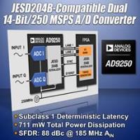
Analog Devices' AD9250 is a dual, 14-bit ADC with sampling speeds of up to 250 MSPS. The AD9250 is designed to support communications applications where low cost, small size, wide bandwidth, and versatility are desired.
The ADC cores feature a multistage, differential pipelined architecture with integrated output error correction logic. The ADC cores feature wide bandwidth inputs, supporting a variety of user-selectable input ranges. An integrated voltage reference eases design considerations and a duty-cycle stabilizer is provided to compensate for variations in the ADC clock duty cycle, allowing the converters to maintain excellent performance. The JESD204B high-speed serial interface reduces board routing requirements and lowers pin count requirements for the receiving device.
By default, the ADC output data is routed directly to the two JESD204B serial output lanes. These outputs are at CML voltage levels. Four modes support any combination of M = 1 or 2 (single or dual converters) and L = 1 or 2 (one or two lanes). For dual ADC mode, data can be sent through two lanes at the maximum sampling rate of 250 MSPS. However, if data is sent through one lane, a sampling rate of up to 125 MSPS is supported. Synchronization inputs (SYNCINB± and SYSREF±) are provided. Flexible power-down options allow significant power savings, when desired. Programmable over-range level detection is supported for each channel via the dedicated fast detect pins. Programming for setup and control are accomplished using a 3-wire SPI-compatible serial interface. The AD9250 is available in a 48-lead LFCSP and is specified over the industrial temperature range of −40°C to +85°C. This product is protected by a U.S. patent.
Features| Applications | |
|
|