By STMicroelectronics 1467
TDA2030A is a single-channel audio power amplifier integrated circuit, usually used in audio amplification applications. It is manufactured by STMicroelectronics and is widely used in sound systems, amplifiers, wireless speakers and other audio equipment.
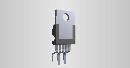
TDA2030A adopts V-shaped 5-pin single-in-line plastic packaging structure. According to the shape of the pin, it can be divided into H type and V type. This integrated circuit is widely used in car stereo radios and medium-power audio equipment. It has the characteristics of small size, high output power and low distortion. And has internal protection circuit. Italian SGS Company, American RCA Company, Japanese Hitachi Company, NEC Company, etc. all produce similar products. Although their internal circuits are slightly different, the pin positions and functions are the same and can be interchanged.
The TDA2030A provides high output current and has very low harmonic and cross-over distortion. Further the device incorporates a short circuit protection system comprising an arrangement for automatically limiting the dissipated power so as to keep the working point of the output transistors within their safe operating area. A conventional thermal shut-down system is also included.
Ⅰ.Working principle of TDA2030A
1.Input stage: The audio signal enters the TDA2030A from the input pin (usually marked as non-inverting input). At this stage, the input signal first passes through a differential amplifier or differential input stage, which helps cancel common-mode noise in the input signal (such as noise from the power supply). This helps improve the anti-interference performance of the audio amplifier.
2.Amplification stage: After passing through the input stage, the audio signal enters the amplifier stage. The TDA2030A uses internal power transistors to amplify the signal. These transistors increase the amplitude of the input signal, thereby providing greater output power. The output signal is passed to an external load, such as a speaker, through an output pin (usually labeled output or non-inverting output).
3.Feedback: TDA2030A usually uses a negative feedback loop to stabilize and control the amplification process. This means that a portion of the output signal is fed back to the input so that it can be compared with the input signal and the amplification level adjusted. This helps reduce distortion and ensures accurate amplification of audio signals.
4.Protection function: TDA2030A usually has overheating protection and short circuit protection functions to ensure that the circuit will not be damaged under extreme conditions. When temperatures rise or a short circuit occurs, these protection features automatically open the circuit to prevent damage.
5.Power supply: TDA2030A usually uses a single power supply. The power pins (usually labeled V+ and V-) are connected to the positive and negative supply voltages to provide the required operating voltage. These voltages will be used to drive the operation of the amplifier.
Ⅱ.Features of TDA2030A
•High sound quality: TDA2030A provides relatively low harmonic distortion and noise levels, enabling high-fidelity audio quality audio amplification.
•Single power supply: TDA2030A can be powered by a single power supply, usually between 6V and 36V, which makes power supply relatively simple.
•Output power: The chip is capable of providing moderate to moderate output power, typically between 5 and 18 watts, making it suitable for many audio and audio applications.
•Built-in protection: TDA2030A integrates overheating protection and short circuit protection functions to protect the circuit from damage such as overheating or short circuit.
•Wide bandwidth: The chip's bandwidth is wide enough to support the amplification of audio signals and is suitable for a variety of audio applications.
•Low cost: The TDA2030A is a relatively affordable solution because of its lower cost and fewer peripheral component requirements.
•Multiple applications: TDA2030A is widely used in various audio applications such as audio systems, power amplifiers, wireless speakers, car audio and home entertainment systems.
•Simplified design: Designing the circuitry associated with the TDA2030A is generally relatively simple because the chip's internal architecture already does most of the amplifier work.
Ⅲ.Typical application diagram of TDA2030A
Ⅳ.TDA2030A pin layout
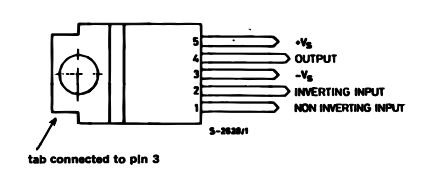
•Pin1: Non-inverting input terminal
•Pin2: Reverse input terminal
•Pin3: Negative power input terminal
•Pin4: is the power output terminal
•Pin5: is the positive power input terminal
Ⅴ.Precautions for TDA2030A
1.Thermal protection: Thermal limit protection has the following advantages. It can easily withstand output overload (even for a long time) or protect when the ambient temperature exceeds.
2.TDA2030A has a load discharge voltage kickback protection circuit. If the peak voltage of the power supply voltage is 40V, then an LC filter must be inserted between pin 5 and the power supply. The diode limits the voltage (pin 5 generates high voltage for any reason, usually The coil inductance of the speaker makes the voltage equal to the voltage of the power supply) to ensure that the pulse train on pin 5 is maintained within the specified amplitude.
3.Compared with ordinary circuits, the heat sink can have a smaller safety factor. In case the junction temperature exceeds, the device will not be damaged. If this happens, Po and Io will be reduced.
4.No insulation is required between the heat sink and the heat sink during assembly, the lead length should be as short as possible, and the welding temperature should not exceed 260°C for 12 seconds.
5.When designing the printed circuit board, the decoupling of the ground wire and the output must be well considered, because these lines have large currents flowing through them.
6.Although TDA2030A requires very few components, the components selected must be of guaranteed quality.
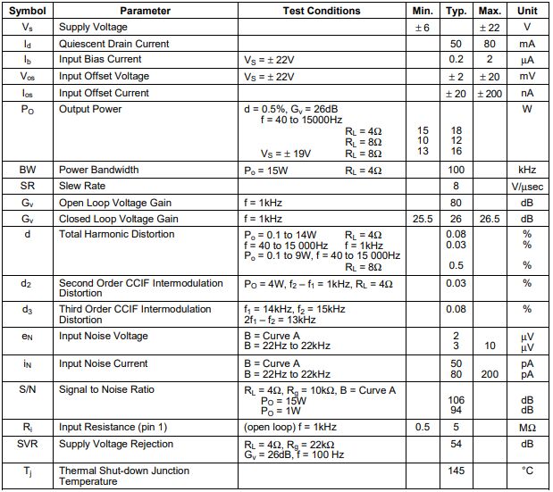
Ⅵ.ELECTRICAL CHARACTERISTICS of TDA2030A
(Refer to the test circuit, Vs=±16V, Tamb=25℃ unless otherwise specified)
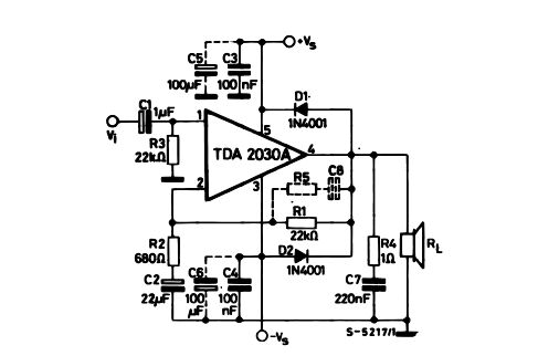
Ⅶ.TDA2030A power amplifier circuit tutorial
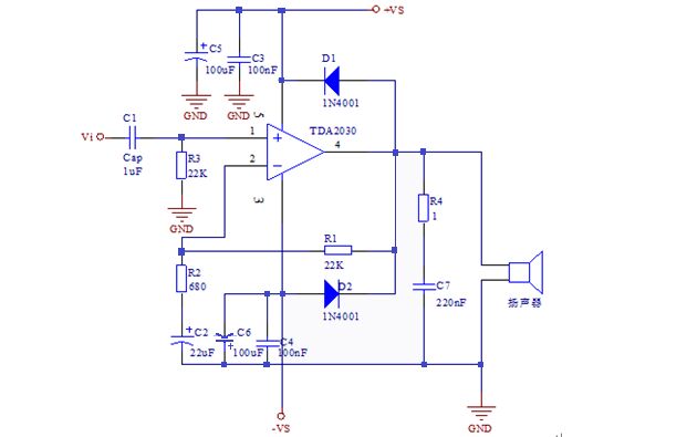
•This circuit is a power amplifier made using op amp TDA2030A. The power supply voltage is ±12V to ±22V, and the maximum output power is 18W.
•This circuit is a deep negative feedback circuit, and the amplification factor of the output voltage is approximately Av=R1/R2=32.3 (please refer to the negative feedback section of the analog electronics book for specific amplification factors). Among them, R4 uses a high-power cement resistor because the current flowing through R4 will be too large when it is no-load. D1 and D2 are diodes, and the one with black or silver wire is the negative pole. Capacitors without positive and negative signs are non-polar capacitors. It is not necessary to distinguish between positive and negative poles. Capacitors marked with positive and negative poles should be distinguished from positive and negative. Be especially careful with capacitors marked with positive and negative poles, as capacitors may explode if they are connected incorrectly.
•The integrated operational amplifier chip TDA2030A has 5 pins, which are: 1. Positive input terminal 2. Inverting input terminal 3. Negative terminal of power supply 4. Output terminal 5. Positive terminal of power supply. When the signal is input from the non-inverting input terminal, the amplified signal at the output terminal is in the same phase as the non-inverting input terminal; when the signal is input from the inverting input terminal, the amplified signal at the output terminal is in opposite phase to the inverting input terminal. Pins 5 and 3 are connected to the power supply respectively. The positive and negative terminals are connected to provide energy for the op amp.
•The size of the signal V can be adjusted by the potentiometer, and then the signal Vi is input from the positive input terminal of pin 1. After input from the rear pin 1, the signal Vi passes through C1 (the function of capacitor C1: intercepts the DC voltage at the positive input terminal). When the signal arriving at the non-inverting input terminal of TDA2030 is input from the non-inverting input terminal (only the AC component is input), the amplified signal at the output terminal has the same phase as the non-inverting input terminal). After the action of TDA2030, the signal is output from pin 4, and the output signal has been amplified. After passing through the action of capacitor C2 (the function of capacitor C2 is to isolate the DC component), the output drives the load.
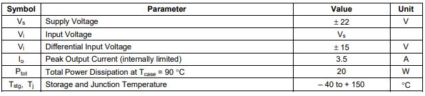
Ⅷ.Absolute Maximum Ratings of TDA2030A
Frequently Asked Questions
1.What is the function of TDA2030A?
The TDA2030A provides high output current with very low harmonic and crossover distortion. The device incorporates a short-circuit protection system that includes means to automatically limit the power dissipated in order to maintain the operating point of the output transistor within its safe operating range.
2.What is the minimum gain of TDA2030?
The TDA2030 has a gain range of 20dB to 60dB.
3.What are the alternative models of TDA2030A?
TDA2050, LM1875, LM386, TA2020, TDA7294, LM1875
4.What are some typical applications of TDA2030A?
TDA2030A is commonly used in applications such as audio amplifiers, home theater systems, wireless speakers, and car audio systems.
5.What are some considerations when designing a circuit with TDA2030A?
When designing a circuit with TDA2030A, consider the power supply requirements, input and output connections, feedback mechanisms, and protection features.